Lab 4
Lab 4: Binary to BCD Converter, Up/Down Counter, and Button Synchronizers
Starts: Week 9 (Oct 15 - Oct 19)
Demo Due: Week 10 (Oct 22 - 26)
Code Due: Friday, Oct 26, 11:59 PM
Points: 150
Pre-Lab Assignment
Create a design for the 5-bit Up/Down Counter and a design the Binary to BCD Converter as described below. Identify which datapath components are needed and how those components will be connected to implement the desired functionality. (10 points)
Code-Check Requirement
An initial implementation for all Verilog modules and testbenches required for the 5-bit Up/Down Counter must be shown to your TA at the beginning of your scheduled lab section in Week 10 (Oct 22 - 26). (5 points)
An initial implementation for all Verilog modules and testbenches required for the Binary-to-BCD Converter must be shown to your TA at the beginning of your scheduled lab section in Week 10 (Oct 22 - 26). (5 points)
Files
- ASCII Displayer Component (ASCII_Displayer.v)
- 50MHz to 200KHz Clock Divider Component (ClkDiv200KHz.v)
- Top Module (BCD_Counter_Top.v)
- Skeleton Verilog Module for Binary to BCD Converter (Binary_BCD_Converter.v)
- Skeleton Verilog Module for 5-bit Up/Down Counter (UpDownCounter_5bit.v)
- Skeleton Verilog Module for Binary To ASCII Decoder (Binary_To_ASCII_Decoder.v)
- Button Synchronizer (Button_Pulse.v)
- LCD Interface Component (LCD_Interface.v)
- PS2 Mouse FSM Component (Lab4_ps2_FSM.v)
- PS2 Mouse Interface Component (Lab4_ps2_Interface.v)
- PS2 Mouse Output Component (Lab4_ps2_Output.v)
- PS2 Mouse Shifter Component (Lab4_ps2_Shifter.v)
- PS2 Mouse Timer Component (Lab4_ps2_Timer.v)
- PS2 Mouse Writer Component (Lab4_ps2_Writer.v)
Lab Overview
In your previous labs, you utilized a binary to ASCII decoder to display a binary number as a hexadecimal number (0 � F). However, as the general public is not likely to be familiar with hexadecimal numbers, we may instead want to display the binary number as a two digit decimal number. In this lab, you will extend your previous design with a 5-bit Up/Down Counter and a Binary to Binary Coded Decimal (BCD) Converter in order to display a 5-bit binary output (ranging from 1 to 20 in decimal) on the LCD of the Spartan-3E FPGA board.
The figure shown below is a top-level view of all necessary components. You will design all components shaded in grey; the others are provided for you. Note that you should use the Binary-To-ASCII decoder and ps2_FSM components designed in your previous labs.
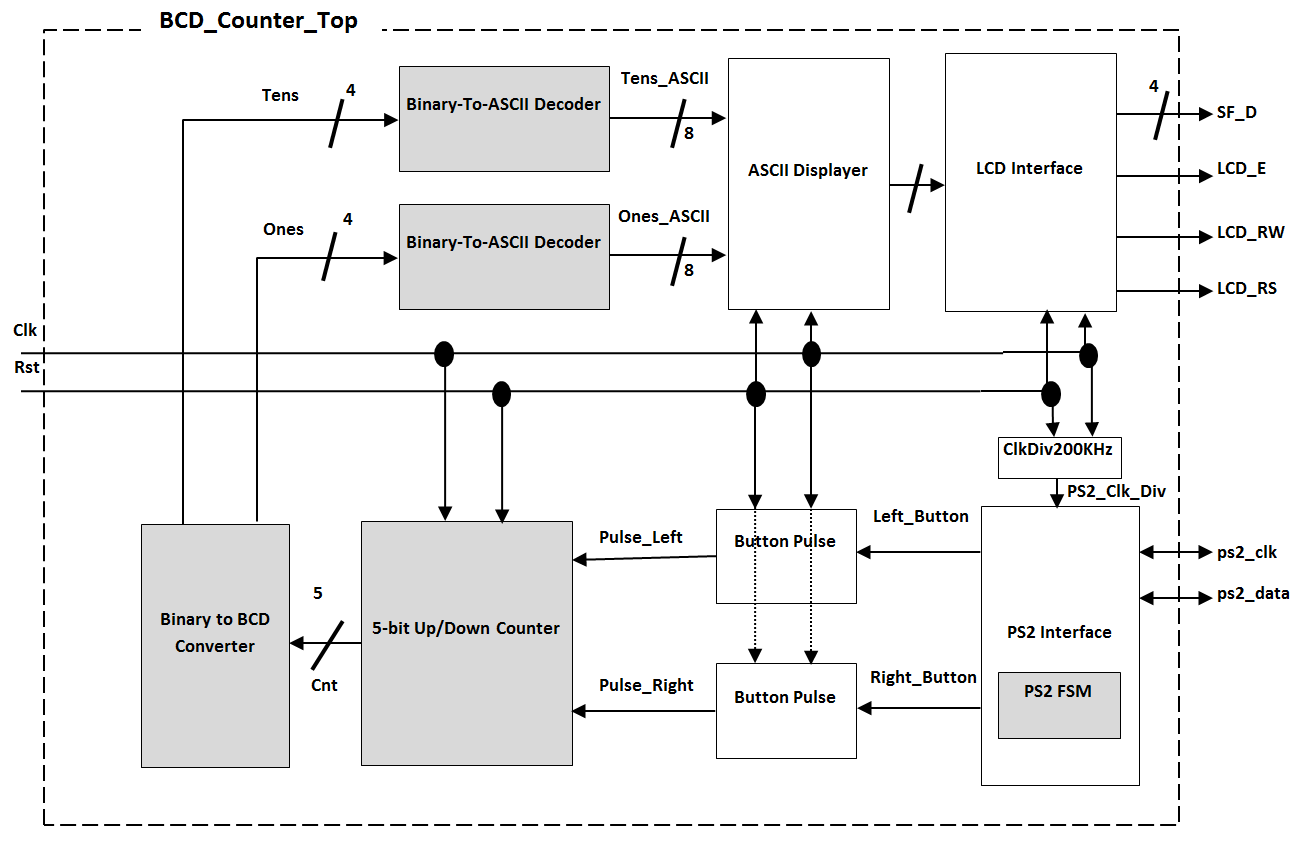
5-bit Up/Down Counter
The 5-bit up/down counter design has four inputs, Clk, Rst, Pulse_Left (left mouse button), Pulse_Right (right mouse button), and a 5-bit output Cnt. If Rst is 1, the counter should reset its count value to zero (0000). If Pulse_Left is 1, the counter should count up. Otherwise, if Pulse_Right is 1, the counter should count down. If both Pulse_Right and Pulse_Left are 0, your counter should remain idle and display the current value. Upon reaching the minimum (0) or maximum (20) count, the counter value should not wraparound. Instead, your counter should continue displaying the current maximum or minimum value until the user choses to count down or up respectively. Lastly, if both Pulse_Left and Pulse_Right are ever 1, your counter should prioritize Pulse_Left and count up.
Binary-to-BCD Converter
In order to display the 5-bit binary number in decimal, you will design a Binary to BCD Converter. A BCD number is a number that uses a 4-bit binary number to represent each decimal digit. For example, the binary number 1111 (15 in decimal), can be encoded as BCD number as 0001 0101. As such, the Binary to BCD Converter has a 5-bit input, Cnt, and two 4-bit outputs, Tens and Ones, corresponding to the binary representation of the tens and ones digit of the decimal equivalent. Given that each output is a binary representation of a decimal digit, the range of possible output values should be 0 to 9.
The above figure provides an overview of the physical connections that will be used to implement your design on the Spartan-3E FPGA board. The overall implementation will have a single Clk input provided by the 50 MHz oscillator integrated on the Spartan-3E FPGA Board, a single reset input, two bidirectional signals for communication with the PS2 mouse, and four outputs for interfacing with the LCD. The following is a constraints (.ucf) file providing the connection details for the inputs and outputs needed for the overall design.
NET "Rst" LOC = "K17" | PULLDOWN;
NET "LCD_E" LOC = "M18" | IOSTANDARD = LVCMOS33 | DRIVE = 4 | SLEW = SLOW ;
NET "LCD_RS" LOC = "L18" | IOSTANDARD = LVCMOS33 | DRIVE = 4 | SLEW = SLOW ;
NET "LCD_RW" LOC = "L17" | IOSTANDARD = LVCMOS33 | DRIVE = 4 | SLEW = SLOW ;
NET "SF_D<8>" LOC = "R15" | IOSTANDARD = LVCMOS33 | DRIVE = 4 | SLEW = SLOW ;
NET "SF_D<9>" LOC = "R16" | IOSTANDARD = LVCMOS33 | DRIVE = 4 | SLEW = SLOW ;
NET "SF_D<10>" LOC = "P17" | IOSTANDARD = LVCMOS33 | DRIVE = 4 | SLEW = SLOW ;
NET "SF_D<11>" LOC = "M15" | IOSTANDARD = LVCMOS33 | DRIVE = 4 | SLEW = SLOW ;
NET "ps2_clk" LOC = "G14" | IOSTANDARD = LVCMOS33 | DRIVE = 8 | SLEW = SLOW | PULLUP ;
NET "ps2_data" LOC = "G13" | IOSTANDARD = LVCMOS33 | DRIVE = 8 | SLEW = SLOW | PULLUP ;
NET "LED<0>" LOC = "F9";
NET "LED<1>" LOC = "E9";
Lab Procedure
- Structurally design the 5-bit Up/Down Counter using any of the following datapath components: adders, subtractors, incrementers, decrementers, multipliers, comparators, shifters, registers, multiplexers, decoders, encoders, and logic gates (only when necessary). Each datapath component used must be modeled behaviorally as a separate Verilog module, and the 5-bit Up/Down Counter must be implemented as a structural connection of those datapath components. Note that you do not need to utilize all components listed above, but rather you are restricted to those components. (50 points)
Note: If you choose to model the entire 5-bit Up/Down Counter behaviorally as one Verilog module (e.g. as an FSM), you will receive a maximum of 25 points.
- Create a testbench to test your design for correct functionality. Your testbench should be self checking using if statements and the $display task to report any errors during simulation. At a minimum, the self checking testbench should test the following cases (10 points):
- Check that the counter counts up then down correctly (2.5 points)
- Check that the counter does not wraparound (2.5 points)
- Check for correct reset behavior from non-one count value (2.5 points)
- Check that the counter continues displaying the current value when both Pulse_Right and Pulse_Left are 0 (2.5 points)
- Create a testbench to test your design for correct functionality. Your testbench should be self checking using if statements and the $display task to report any errors during simulation. At a minimum, the self checking testbench should test the following cases (10 points):
- Structurally design the Binary to BCD Converter using any of the following datapath components: adders, subtractors, incrementers, decrementers, multipliers, comparators, shifters, registers, multiplexers, decoders, encoders, and logic gates (only when necessary). Each datapath component used must be modeled behaviorally as a separate Verilog module, and the Binary to BCD Converter must be implemented as a structural connection of those datapath components. Note that you do not need to utilize all components listed above, but rather you are restricted to those components. (50 points)
Note: If you choose to model the entire Binary to BCD Converter behaviorally as one Verilog module, you will receive a maximum of 25 points.
- Create a testbench to test the Binary to BCD Converter for correct functionality. No specific requirements are needed for the testbench, but you must be able to demonstrate the correctness of your design to your TA. (10 points)
- Synthesize and download your modified design to the Spartan-3E FPGA board using the provided user constraint file and test your design for correct functionality. (30 points)
Hints and Tips
- Be careful of bit width mismatches. You should get warnings from the ISE indicating a problem.