Lab 3
Lab 3: FSM for PS2 Mouse Interface
Starts: Week 6 (Sept 24 – Sept 28)
Demo Due: Week 7 (Oct 1 – Oct 5)
Code Due: Friday, Oct 5, 11:59 PM
Points: 85
Pre-Lab Assignment
Create a state diagram for the 4-bit Up/Down Counter design described below. You do not need to create a truth table or derive equations. (10 points)
Code-Check Requirement
An initial implementation for all Verilog modules and testbenches required for this lab assignment must be shown to your TA at the beginning of your scheduled lab on the week the assignment is due. (5 points)
Files
- Top Module (Lab3_Counter_Top.v)
- Verilog Module for ASCII Displayer (Lab3_ASCII_Displayer.v)
- Verilog Module for the LCD Interface (Lab3_LCD_Interface.v)
- Skeleton Verilog Module for the Binary-To-ASCII Decoder (Lab3_Binary_To_ASCII_Decoder.v)
- Clock Divider (Lab3_ClkDiv.v)
- Skeleton Verilog File for 4bit Up/Down Counter FSM (Lab3_Counter.v)
- Skeleton Verilog File for the PS2 mouse FSM (Lab3_ps2_FSM.v)
- Testbench for the PS2 mouse FSM (Lab3_Testbench_ps2_FSM.v)
- Module to interface with PS2 mouse (Lab3_ps2_Interface.v)
- Module to reconstruct received PS2 mouse data (Lab3_ps2_Output.v)
- Module to shift in data from the PS2 mouse (Lab3_ps2_Shifter.v)
- Timer to detect end of incoming mouse data (Lab3_ps2_Timer.v)
- Module to transmit data to the PS2 mouse (Lab3_ps2_Writer.v)
Lab Overview
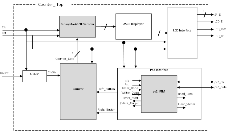
In this lab, you will design two Finite-State Machines in order to display an increasing or decreasing count on the LCD. The figure shown below illustrates a top-level view of the required components. You will only have to design the shaded components; the other components have been provided for you. Note that you should use the Binary-To-ASCII Decoder you designed in the previous lab.
PS2 FSM
You will first design the Finite-State Machine for the PS2 mouse controller in order to allow your design to read data from the mouse. A complete segment of data is delivered from the mouse to the FPGA one bit at a time. Your design will essentially detect each bit and allow the reconstructed data to propagate to the other components once all bits have been received.
This PS2 mouse controller has 6 1-bit inputs, Clk, Rst, ps2_clk, ps2_data, Writer_Done, Timer_Done, and 4 1-bit outputs Timer_Start, Update_Output, Read_Data, and Clear_Shifter. Your FSM design should have the following 6 states: Init, Idle, Clk_Low_Read, Clk_Low_Hold, Clk_High_Timer, and Update. The following discussion describes the functionality of each of the aforementioned states. You should assume that all outputs are 0 in every state unless stated otherwise.
When Rst is 1, the FSM will automatically transition to the Init state. In the Init state all outputs should be set to 0 and a transition to the Idle state should occur when Writer_Done becomes 1 – otherwise your FSM should remain in the Init state. Once in the Idle state, your FSM should wait for both ps2_data and ps2_clk to become 0 before transitioning to the Clk_Low_Read state. The Read_Data output should be set to 1 while in the Clk_Low_Read state, however, your FSM should immediately transition to the Clk_Low_Hold state on the next clock cycle. In the Clk_Low_Hold state, all outputs should be set to 0 and your FSM should remain in this state until ps2_clk becomes 1, resulting in a transition to the Clk_High_Timer state. The Timer_Start output should be set to 1 while in the Clk_High_Timer state, which has three possible transitions. If Timer_Done is 1, the FSM should transition to the Update state. Otherwise, if Timer_Done is 0 and ps2_clk is 0, the next state should be Clk_Low_Read. If none of the previous conditions are met, the FSM should remain in the Clk_High_Timer state. Finally, in the Update state Update_Output should be set to 1 and a transition to the Clk_Low_Read state should occur if ps2_clk is 0. Otherwise, the FSM should return to the Idle state.
4-bit Up/Down Counter
The 4-bit up/down counter design has four inputs, Clk, Rst, LB (left moust button), RB (right mouse button), and a 4-bit output Cnt, represented by the four outputs Cnt3, Cnt2, Cnt1, Cnt0. If Rst is 1, the counter should reset its count value to zero (0000). Otherwise, if LB is 0, on every clock cycle the counter should count up by one number. If LB is 1, the counter should count down on every clock cycle. Upon reaching the minimum (0) or maximum (8) count, the counter value should wraparound. For example, when counting up, the counter should wraparound to 0 after 8, and when counting down, the counter should wraparound to 8 after 0. Lastly, if RB is ever 1, your counter should pause and continue displaying the current count value.
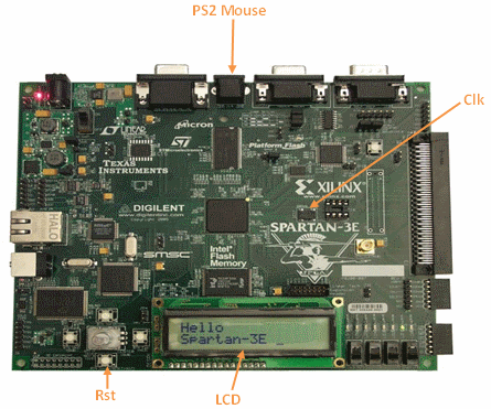
The figure to the right provides an overview of the connections that will be used to implement your 4-bit Up-then-Down Counter on the Spartan-3E FPGA board. The overall counter implementation will have a single Clk input provided by the 50 MHz oscillator integrated on the Spartan-3E FPGA Board, one reset input, and ps2_data and ps2_clk signals provided by the PS2 Mouse. The implementation will also interface with your Binary-To-ASCII Decoder in order to display results to the LCD. The following is a .ucf file providing the connection details for the new inputs and outputs needed for the 4-bit Up-then-Down Counter:
NET "Rst" LOC = "K17" | PULLDOWN;
NET "DivRst" LOC = "D18" | PULLDOWN;
NET "ps2_clk" LOC = "G14" | IOSTANDARD = LVCMOS33 | DRIVE = 8 | SLEW = SLOW | PULLUP ;
NET "ps2_data" LOC = "G13" | IOSTANDARD = LVCMOS33 | DRIVE = 8 | SLEW = SLOW | PULLUP ;
NET "LCD_E" LOC = "M18" | IOSTANDARD = LVCMOS33;
NET "LCD_RS" LOC = "L18" | IOSTANDARD = LVCMOS33;
NET "LCD_RW" LOC = "L17" | IOSTANDARD = LVCMOS33;
NET "SF_D<8>" LOC = "R15" | IOSTANDARD = LVCMOS33;
NET "SF_D<9>" LOC = "R16" | IOSTANDARD = LVCMOS33;
NET "SF_D<10>" LOC = "P17"| IOSTANDARD = LVCMOS33;
NET "SF_D<11>" LOC = "M15"| IOSTANDARD = LVCMOS33;
NET "LED<0>" LOC = "F9";
NET "LED<1>" LOC = "E9";
Lab Procedure
- Behaviorally design the PS2 mouse Finite State Machine (FSM). Your FSM should adhere to the guidelines presented in the above discussion and pass all test cases within the provided testbench file. (15 points)
- Behaviorally design the 4-bit Up/Down Counter as a Finite State Machine. Your FSM design should consist of two always procedures. The first always procedure, should implement the state register. The second always procedure should implement the FSM control logic. In the design of the FSM control logic, you must use a case statement to describe the combinational behavior associated with each state. (20 points)
- Create a testbench to test your design for correct functionality. Your testbench should be self checking using if statements and the $display task to report any errors during simulation. At a minimum, the self checking testbench should test the following cases (20 points):
- Check that counter counts up then down correctly (5 points)
- Check for correct wraparound functionality for counting up and down (5 points)
- Check for correct reset behavior from non-one count value (5 points)
- Check for correct pause behavior (5 points)
- Synthesize, download and test your design on the Spartan-3E FPGA board for correct functionality. At a minimum, you should test the same cases as your self checking testbench. (15 points)