Lab 4: Binary to BCD Converter and Multiplexed BCD Display Driver
Starts: Week 8 (Oct 12-Oct 16)
Demo Due: Week 10 (Oct 26-Oct 30)
Code Due: Friday, Oct 30, 11:59PM
Points: 150
Pre-Lab Assignment
Create a design for the Binary to BCD Converter and Refresher components described below, specifically identifying which datapath components are needed and how those components will be connected to implement the desired functionality. (10 points)
Code-Check Requirements
An initial implementation for all Verilog modules and testbenches required for the Binary-to-BCD Converter must be shown to your TA at the beginning of your scheduled lab section during Week 9 (Oct 19-Oct 23). (5 points)
An initial implementation for all Verilog modules and testbenches required for the Refresher must be shown to your TA at the beginning of your scheduled lab section during Week 10 (Oct 26-Oct 30). (5 points)
Files
- 7-segment Display Datasheet (Digilent Pmod SSD)
- User Constraint File (Lab4_Top.ucf)
- State Machine for Rotary Counter (Lab4_RotaryCounter.v)
- Skeleton Verilog Module for Binary to BCD Converter (Lab4_Binary2BCD.v)
- Skeleton Verilog Module for Multiplexed BCD Display Driver (Lab4_BCDDispDriver.v)
- Skeleton Verilog Module for Refresher (Lab4_Refresher.v)
Lab Overview
In your previous labs, you utilized a binary to 7-segment LED decoder to display a binary number as a hexadecimal number. However, as the general public is not likely to be familiar with hexadecimal numbers, we may instead want to display the binary number as a two digit decimal number using the two 7-segment LED displays. In this lab, you will design a Binary to Binary Coded Decimal (BCD) Converter and a Multiplexed BCD Display Driver to display a 5-bit binary output (ranging from 1 to 20 in decimal) from a Rotary Counter on the two 7-segment displays connected to the Spartan-3E FPGA board.
Binary-to-BCD Converter
In order to display the 5-bit binary number in decimal, you will first design a Binary to BCD Converter. A BCD number is a number that uses a 4-bit binary number to represent each decimal digit. For example, the binary number 1111 (15 in decimal), can be encoded as BCD number as 0001 0101. As such, the Binary to BCD Converter has a 5-bit input, Cnt, and two 4-bit outputs, Tens and Ones, corresponding to the binary representation of the tens and ones digit of the decimal equivalent.
Multiplexed 2-digit BCD Display Controller
In designing the binary to 7-segment LED decoder in Lab 2, the SegSel output was used to control which 7-segment LED display would be utilized to display the 4-bit binary number. As such, we cannot simultaneously display a digit on both 7-segment LED displays. Instead, by repeatedly and continuously display a digit on each display faster than the human eye can respond, both displays will appear to be illuminated at the same time. In this lab, you will also design and build a Multiplexed BCD Display Driver to display the Tens and Ones outputs of the Binary to BCD Converter on the corresponding 7-segment LED displays. The Multiplexed BCD Display Driver builds upon your binary to 7-segment decoder by adding a refresher circuit to control when each 7-segment display will be illuminated and a multiplexer to select between the Tens and Ones output of the Binary to BCD Converter. The following provides an overview of the multiplexed BCD to 7-segment display driver.

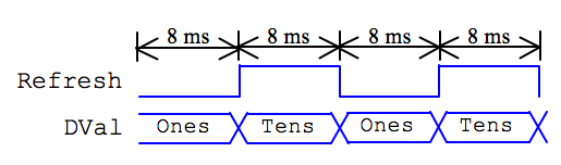
For the 7-segment LED display connected to the Spartan-3E FPGA board, each 7-segment LED display should be illuminated for 8 ms, as illustrated in the following timing diagram. Given the 50 MHz clock provided by the Spartan-3E FPGA board, the Refresher circuit should generate an oscillating output, Refresh, that remains 1 for 8 ms, 0 for 8 ms, and repeats. The Refresh output will be used to control the SegSel output and as the select line to the multiplexer for selecting which BCD digit will be the input to your Binary to 7-segment LED Decoder. Please note that you will need to modify your Binary to 7-segment LED Decoder to remove the SegSel output, as the SegSel signal will be connected to the Refresh output of the Refresher circuit.
The final implementation will utilize a Rotary Counter component provided with this lab assignment. As you turn the rotary switch on Spartan-3E board, the Rotary Counter will increment or decrement a 5-bit Cnt output from a minimum decimal value of 1 to a maximum decimal value of 20.
Lab Procedure
- Structurally design the Binary to BCD Converter using any of the following datapath components: adders, subtractors, incrementers, decrementers, multipliers, comparators, shifters, registers, multiplexers, decoders, encoders, and logic gates (only when necessary). Each datapath component used must be modeled behaviorally as a separate Verilog module, and the Binary to BCD Converter must be implemented as a structural connection of those datapath components. Note that you do not need to utilize all components listed above, but rather you are restricted to those components. (50 points)
Note: If you choose to model the entire Binary to BCD Converter behaviorally as one Verilog module, you will receive a maximum of 25 points.
- Create a testbench to test the Binary to BCD Converter for correct functionality. No specific requirements are needed for the testbench, but you must be able to demonstrate the correctness of your design to your TA. (10 points)
- Design the Multiplexed BCD Display Driver and Refresher sub-components. The Multiplexed BCD Display Driver and Refresher sub-components must be modeled structurally (as described above) for full credit. If either of these components are modeled behaviorally, you will receive one half of the possible points. (50 points).
Note: You will need to accurately describe how your Refresher component works to your TA to receive full points.
Note: If you choose to model the Multiplexed BCD Display Driver and Refresher sub-components behaviorally , you will receive a maximum of 25 points.
- Create a testbench to test the Multiplexed BCD Display Driver for correct functionality for one full refresh period. Due to the memory limitations of the computers within the ECE 274 Laboratory, you should test your design assuming a refresh period is 16 us (instead of 16 ms). Be sure to correct your design before synthesizing the circuit to the Spartan-3E FPGA board. (10 points)
- Create a top-level component that structurally connects the Rotary Counter, your Binary to BCD Converter, and your Multiplexed BCD Display Driver. Synthesize and download your modified design to the Spartan-3E FPGA board using the provided user constraint file and test your design for correct functionality. (30 points)