Lab 5: Reaction Timer
Starts: Week 12 (Nov 10-Nov 14)
Demo Due: Week 15 (Dec 01-Dec 05)
Code/Report Due: Friday, Dec 05, 11:59PM
Points: 150
Pre-Lab Assignment
Create a high-level state machine (HLSM) diagram for the Reaction Timer design describe below. Be sure to use the same inputs and outputs as specified in the following description. (20 points)
Lab Report
A lab report is required for this lab assignment using the provided template, ECE 274 Lab Report Template. Only one lab report is required for each group. In addition to following the specified lab report template, your lab report should include a figures for your final high-level state machine diagram and simulation waveforms demonstrating correct functionality of the Reaction Timer and RandomGen components. The lab report must be submitted via D2L as a Word or PDF file along with your code submission. (10 points)
Files
- ZIP Archive of all Verilog files for Extra Credit Lab
- Top Level Design Module (Lab5_Top.v)
- User Constraint File (Lab5_Top.ucf)
- Clock Divider for LCD Interface (Lab5_LCDClkDiv.v)
- LCD Display Controller Module (Lab5_LCDDisplay.v)
- LCD Interface Module (Lab5_LCDInterface.v)
- 10-bit Binary to 4 Digit BCD Converter (Lab5_Bin2BCD.v)
- Skeleton Verilog Module for Reaction Timer (Lab5_ReactionTimer.v)
- Skeleton Verilog Module for RandomGen (Lab5_RandomGen.v)
- Skeleton Verilog Module for ClkDiv (Lab5_ClkDiv.v)
Lab Overview
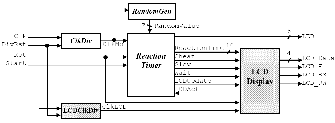
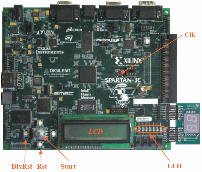
In this lab, you will be designing a Reaction Timer that measures a user’s reaction time by measuring the time elapsed between illuminating a set of LEDs and the pressing of a button by a user. On reset, the Reaction Timer will initially display an introduction message “Reaction Timer” on the LCD of the Spartan-3E FPGA board. When the Start button is pressed, the reaction timer will wait for a random length of time between 2 and 4 seconds while displaying “Wait for LEDs...” on the LCD. The reaction timer will then illuminate all eight of the individual LEDs of the Spartan-3E FPGA board and measure the length of time in milliseconds before the user presses the Start button again. The measured reaction time will be displayed on the LCD display in the following format: “0.345 s”. If the user did not press the Start button within .999 seconds (999 milliseconds) of illuminating the LEDs, the reaction timer will display “Too Slow!” on the LCD. Alternatively, if the user pressed the Start button before illuminating the LEDs, the reaction timer will display “No Cheating!” on the LCD. The Reaction Timer will continue to display the last recorder reaction time, cheat message, or slow message, until the user pushes the Start button to perform a new measurement. The following figures provide a top level view of the various components of the Reaction Timer you will be designing and provide an overview of the connections that will be used to implement your Reaction Timer on the Spartan-3E FPGA board. The shaded components are predesigned components provided to you that you must interface with to implement the Reaction Timer design. The top level component (Lab5_Top.v) and User Constraint File (Lab5_Top.ucf) are available on the course webpage.
Reaction Timer
The Reaction Timer component provides the main functionality of the overall design and will interface with the clock divider (ClkDiv), the random number generator (RandomGen), and the LCD display (LCDDisplay). In this lab, you will create an RTL design of the above specified reaction timer as high-level state machine (HLSM). The Reaction Timer component has four inputs, ClkMS, Rst, Start, and LCDAck, and six outputs, LED, ReactionTime, Cheat, Slow, Wait, and LCDUpdate.
The ClkMS input is a 1kHz clock signal generated by the ClkDiv component. While the Reaction Timer’s HLSM could directly operate using the 50MHz clock provided by Spartan-3E FPGA board, a 1Khz clock signal provide a simplified method for counting the elapsed time in milliseconds – 1 clock cycle of a 1 kHz clock is equal to 1 millisecond. You will need to design the ClkDiv component that will generate a 1 kHz clock output, ClkMS, from the 50 MHz clock input provided by Spartan-3E FPGA board
The RandomValue input is an N-bit number output from the RandomGen component that provides a random value between 2 and 4 seconds used to delay the illumination of the LEDs for a random length of time. As there are many ways to design the RandomGen component, the number of bits used to represent the RandomValue signal is not defined. Instead, in designing the RandomGen component, you will need to determine the number of bits needed for this value. The RandomGen component need not implement a true random number generator, or pseudo-random number generator. Instead, the RandomValue should appear to be random when read by the Reaction Timer at the appropriate time. Please note that the built-in Verilog function $random is not synthesizable and should not be used. Hint: this circuit may be much simpler than you might first anticipate.
The LED output is an 8-bit output that will connect to the eight individual LEDs available on the Spartan-3E FPGA board. The Reaction Timer should illuminate all eight LEDs to indicate that the user should press the Start button as soon as possible. In all other circumstances, the LEDs should not be illuminated.
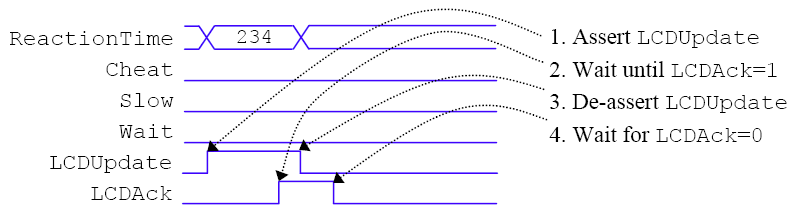
The input LCDAck and outputs ReactionTime, Cheat, Slow, Wait, and LCDUpdate are used to interface with the provided LCDDisplay component. The ReactionTime output is a 10-bit output that corresponds to the measured time in milliseconds of a successful reaction time measurement. The Cheat output is a one bit output indicating the user pressed the Start button before the LEDs were illuminated and the “No Cheating!” message should be displayed on the LCD. The Slow output is a one bit output indicting the user did not press the Start button within 1 second after illuminating the LEDs and the “Too Slow!” message should be displayed on the LCD. The Wait output is a one bit output indicting that the “Wait for LEDs...” message should be displayed on the LCD. Finally, the LCDUpdate output and LCDAck input are used for communicating with the LCDDisplay component to specify when and how the LCD display should be updated. Because the LCDDisplay and Reaction Timer components operate using two different clock signals, in order to communicate between the two components, your design will have to implement a simple handshaking scheme. As illustrated in the following timing diagram, to update the LCD, the Reaction Timer must first assert the LCDUpdate output and continue to assert this output until the LCDAck input is asserted by the LCDDisplay component. Upon detecting that the LCDAck input is high, the Reaction Timer must de-assert the LCDUpdate signal and wait for the LCDAck input to be de-asserted as well. This handshaking sequence is required for all updates to the LCDDisplay. For example, to display a measured reaction time on the LCD, the Reaction Timer should assign the measured reaction time in milliseconds to the ReactionTime output, assign 0 to Cheat, Slow, and Wait, assert the LCDUpdate output, and complete the handshaking as described above. Note that the values assigned to ReactionTime, Cheat, Slow, and Wait must remain constant as long as LCDUpdate is asserted. As another example, to display the wait message on the LCD, the Reaction Timer should assign 1 to the Wait, assign 0 to Cheat and Slow, assert the LCDUpdate output, and complete the handshaking as described above.
The provided top-level module (Lab5_Top.v) integrates the various components together to implement the overall reaction timer design. In designing the Reaction Timer, RandomGen, and ClkDiv components, be sure to use consistent module names to ensure your components will integrate effortlessly. Skeleton Verilog modules are also provided for the Reaction Timer (Lab5_ReactionTimer.v), RandomGen (Lab5_RandomGen.v), and ClkDiv (Lab5_ClkDiv.v) components.
Lab Procedure
- Behaviorally design the ReactionTimer and RandomGen components (75 points):
- Behaviorally design the ReactionTimer as a high-level state machine using either a one-procedure or two-procedure implementation. Note: If you choose to utilize a two-procedure implementation for your high-level state machine, be sure to model all registers within your design using separate current and next reg variables. The following is the breakdown in points awarded for various elements of the ReactionTimer design. (50 points)
- Measuring reaction time in milliseconds. (20 points)
- Interfacing with LCD to display messages. (15 points)
- Detecting cheat condition. (5 points)
- Detecting slow condition. (5 points)
- Waiting for random length of time provided by the RandomValue input. (5 points)
- Behaviorally design the RandomGen component using any implementation style. Hint: The RandomGen component need not explicitly generate subsequent random numbers, but rather should appear to be random with respect to the user’s interactions with your design. (10 points)
- Create a testbench that connects the Reaction Timer and RandomGen components to test your Reaction Timer design for correct functionality. Your testbench should check for correct reaction time measurement, correct cheating detection, and correct slow reaction detection. Note: As you are not yet interfacing with the LCDDisplay component, you will need to control the LCDAck signal from within your testbench to provide and acknowledge in response to the LCDUpdate signal. (15 points)
- Behaviorally design the ReactionTimer as a high-level state machine using either a one-procedure or two-procedure implementation. Note: If you choose to utilize a two-procedure implementation for your high-level state machine, be sure to model all registers within your design using separate current and next reg variables. The following is the breakdown in points awarded for various elements of the ReactionTimer design. (50 points)
- Design the clock divider, ClkDiv. (15 points)
- Design the clock divider, ClkDiv, that outputs a 1kHz clock from the 50 MHz clock input provided on the Spartan-3E FPGA board. Note: You may design the clock divider behaviorally (similar to the ClkDiv component provided in Lab 3). (10 points)
- Create a testbench to test your ClkDiv component for one full clock period (1 millisecond). (5 points)
- Using the provided top level module (Lab5_Top.v) and User Constraint File (Lab5_Top.ucf), synthesize, download, and test your overall reaction timer design on the Spartan-3E FPGA board. Note: As most information is provided through the LCD for this assignment, you must minimally be able to interface with the LCD and display a message other than introduction message “Reaction Timer” on the LCD. (30 points)