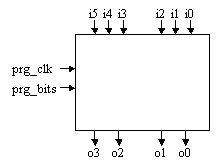
In this lab, you will design a simple Configurable Logic Block (CLB), which is an integral part of modern FPGAs. While CLBs incorporated into commercially available FPGAs range in complexity and size, a common aspect among most these CLBs is the use of look-up tables (LUT) for implementing logic functions. Additionally, CLBs often consist of multiple LUTs along with programmability allowing LUTs to be connected together within the CLB. You will be designing a simple CLB consisting of two 3-input 2-output LUTs. The following figure provides a black box view of the CLB design, consisting of 6 inputs and 2 outputs connected to the internal LUTs and two programming inputs (prg_clk and prg_bits) used to load the bitstream to program the CLB.
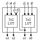
The following figure provides the internal details of the CLB. As mentioned earlier,
the CLB is composed of two 3-input 2-output LUTs. Additionally, output o1 from
the right LUT can optionally be connected to input i3 of the left LUT.
Note: This figure does not provide any details regarding the required resources
and connections need to support programming the CLB. You will be responsible for determining
and designs the required elements.
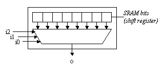
As shown in the figure below, depicting a 3-input 1-output LUT, a LUT is comprised of SRAM cells to store the contents of the LUT and a multiplexor to select the LUT element based on the inputs to the LUT. To support programming a CLB using a bitstream, the LUT SRAM cells correspond to the SRAM shift register you designed in a previous lab.
After designing the CLB, you will also be required to program your CLB design to implement a 2-bit ripple-carry adder with a carry-in and carry-out. Furthermore, you must also configure your CLB to implement the following logic functions.
f = ab'c'd + a'cd + d'e
g = a'b + ac
The following provides the steps that you must follow to complete this lab. While the following steps provide the larger milestones you will need to achieve in order to complete this lab, you may want to design and test smaller aspects of your LUT and/or CLB designs individually.
You must demo the following aspects or your CLB design to the TA.
In addition to the standard lab report format, you must submit the following information.