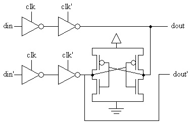
In this lab, you will design a 4-bit shift SRAM-based shift register. While many different shift register design exist, an SRAM-based shift register is useful due to the property that the contents of the register are retained without the presence of a clock signal. The following figure presents the design of a 1-bit SRAM shift register cell.
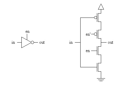
The individual shift register cell is composed of an SRAM cell along with 4 tri-state inverting buffers. The design of the tri-state inverting buffer is provided in the following figure.
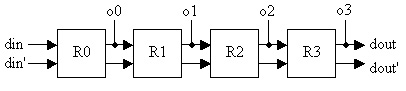
Finally, the individual shift register cells will be connected together as shown in the following diagram to create the 4-bit SRAM shift register.
This lab is the second of three labs that will culminate in the design of simple Field Programmable Gate Array (FPGA). Therefore, you should work very diligently to ensure you complete this lab on-time.
Note: In designing your shift register, be careful with your initial 1-bit shift register layout, as when designing the 4-bit shift register, you will not only need to serially connect the 1-bit shift register cells, but you will also need to route the global clock signals to all cells.
The following provides the steps that you must follow to complete this lab.
You must demo the following aspects or your 4-bit SRAM shift register design to the TA.
In addition to the standard lab report format, you must submit the following information.