Lab/Tutorial 1 - Introduction to Cadence Schematic Capture and Simulation
In this course, we will use the Cadence design tools to design schematics and
layouts of various hardware designs. These tools are the state-of-the-art CAD
tools widely used in industry. The Cadence tools provide many features and functionality,
some of which you will not need in this course. This tutorial will provide a
basic introduction on how to use the schematic capture and simulation tools
along with various other helpful functions.
Cadence Setup and Initialization
- Log onto hercules.cs.ucr.edu using puTTY (or other ssh program).
- Execute the following commands:
source /usr/local/cadence/usecadence/
export DISPLAY=yourMachineIP:0
- Download cds.lib to your home directory, and copy the file to the location /cadence/login
- Before using Cadence for the first time, we need to create directories in which Cadence will store the
design we create. While you can store the designs in any location, this tutorial assumes you will be using the
location cadence/mylibs. To create this directory execute the following commands:
cd
mkdir cadence
mkdir cadence/mylibs
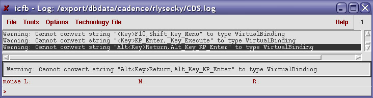
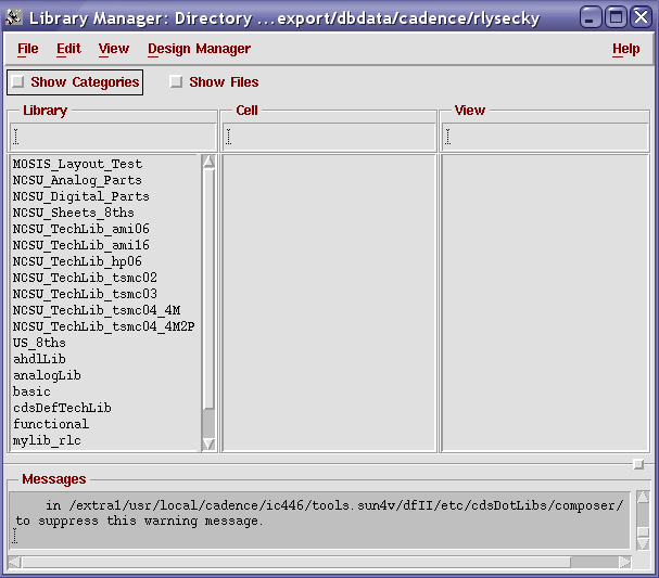
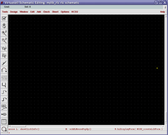
- Execute the command icfb& to start Cadence.
You should be presented with the Command Interpreter Window (CIW) and Library Manager windows as shown below:
Note: When you exit the Cadence design environment not all processes
started by the application will be stopped. Unless you ensure that you kill
all cadence processes when you exit, hercules will become slower and less responsive.
When you are finished using Cadence or if Cadence crashes on you, please make
sure to kill your processes. To kill all Cadence processes, run the following
command:
ps -ef | grep $logname | grep cadence | awk '{print $2}' | xargs kill -9
In addition, at 2AM everyday, all Cadence processes will automatically be terminated. If you are working on your lab around
that time frame, please make sure you save all of your work.
Library Creation
It is strongly recommended that you create a library for each tutorial or lab
assignment using a descriptive library name. The create a library for the tutorial,
use the following procedure as shown below:
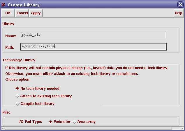
- Using the Library Manager Window, select File => New => Library.
- Enter the library name mylib_rlc in the Name field.
- Enter the path ~/cadence/mylibs in the Path field.
- Select the option No tech library needed under Technology Library.
- Click OK.
Creating a New Design
During the curse of each lab assignments, you will have to create several designs, including schematics, layouts
and test circuits. For each of these items, you can create the designs using the following procedure as shown below:
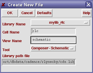
- Using the Library Manager Window, select File => New => Cell View.
- Select mylib_rlc from the Library Name drop-down menu.
- Enter the cell name rlc in the Cell Name field.
- Enter the view name schematic in the View Name field.
- Select Composer-Schematic from the Tool drop-down menu.
Schematic Capture
You should be presented with a empty Composer window as shown:
Cadence provides many different ways for adding components to your schematic
and/or changes options. While designing a circuit, you can use the menus, toolbar
(icons on the left side of the screen), or keystroke to accomplish the same
task. If you use the toolbar, as you move the mouse over each toolbar icon,
a popup description will indicate the functionality.
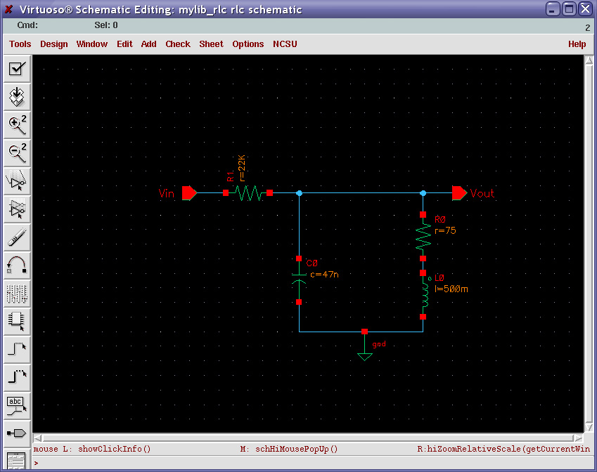
To demonstrate how to create a schematic design, we will be designing the circuit
shown here.
Adding Component Instances
- Click on the Instance icon or select Add => Instance.
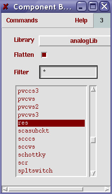
- You will be presented with two windows, the Component Browser and the Add Instance windows.
- From the Component Browser Window, under Library, select analogLib.
- Click on the Flatten checkbox, to provide the full list of components available in this library.
- Select the component res from the list. By selecting the resistor component,
the corresponding information will be filled in the Add Instance window.
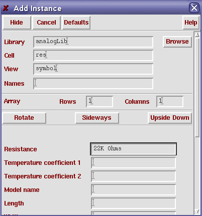
- The Add Instance window will also allow us to customize the component we
are adding to our schematic. In this case, we would like to adjust the value
of the resistor we are adding to 22 K Ohms. As shown below, we simply enter
the desired value into the Resistance field.
- Within the schematic editing window, as you move the mouse you should see the outline of a resistor.
Place two resistor within your schematic as shown in the completed schematic shown above.
- Using the same procedure, add a 47n F capacitor, cap, as shown in the completed schematic.
- Using the same procedure, add a 500m H inductor, ind, as shown in the completed schematic.
- Using the same procedure, add a ground, gnd, as shown in the completed schematic.
- When completed, to exit the Add Instance mode, close the Add Instance window
and within the schematic editing window hit Escape. Similarly, when editing
a schematic or layout, to deselect a given tool, you can simply hit the Escape
key.
- In order to rotate a component instance, you can either select the component by clicking and press
r or you select the component and select Edit => Rotate.
Adding IO Pins
We now need to add IO pins to your design using the following procedure.
- Click on the Pin icon or select Add => Pin. You will be presented with the
Add Pin dialog as shown here.
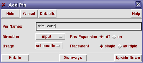
- Under the Pin Names field, enter Vin Vout.
- We will initially select the Direction as Input.
- Within the schematic window, place the first pin, Vin as shown in the completed schematic. After
placing the first pin, you should notice that the Pin Names field in the Add Pin window
now only contains, Vout.
- We now need to change the pin Direction to Output and place the Vout
as shown in the completed schematic.
Connection Wires
Now that all of our components and IO pins have been added we need to connect the components together
with wire. To connect components within wire, use the following procedure.
- Click on the Wire icon or select Add => Wire (narrow). You will be presented with the
Add Wire dialog as shown here.
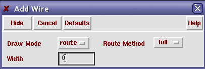
- Within the schematic editing window, draw wires by selecting a starting
point and dragging the mouse to the desired endpoint. You can create wires
to connect components together, to connect two existing wires together, and
connecting a component to existing wire.
Modifying Instance Properties
We often will need to change the properties of a component we have added to a design. While we could
simply delete the component and add the correct component, we can also modify the properties directly.
- You currently should have two 22K Ohm resistors in your design. However, looking at the
completed schematic, the vertical resistor on the right should be 75 Ohms instead.
- Select the resistor by clicking on it once.
- Click on the Properties icon, select Edit => Properties =>
Object, or press the q key. You will be presented with the Edit
Object Properties window as shown here.
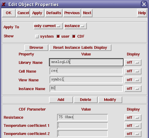
- Modify the Resistance to 75 Ohms and click on OK.
Saving your Designs
While you can simply save your design by click on the Save icon or selecting Design => Save,
there is a better way to save you designs use the Check and Save.
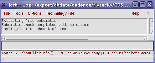
- Select Design => Check and Save. This option will check you design for any
errors or warnings that may be present.
- You will notified of errors by a visual indicator within your design as well as the error or warnings
information within the CIW window. If you created your schematic properly, you should see the following message in
the CIW window shown here.
- If you have errors, you will see small flashing squares within the schematic editing window.
- Read the error and warning messages within the CIW windows and the correct the errors/warnings
as necessary.
- Once correct, check and save your design by selecting Design => Check
and Save.
Quick Usage Reference
the following are some keyboard shortcuts for commonly used commands.
- Press p to add pins.
- Press q to after selecting a component to edit properties.
- Press w to add wires.
- Press f to fit the schematic to the schematic window.
- Press l to label a wire.
- Press Up or Down arrow to scroll your design.
- Press ESC to terminate any of the operation within the schematic window.
Printing a Design
For all of your labs, you will need to turnin printouts of the designs you created. In order to print
your schematic, use the following procedure.
- Select Design => Plot => Submit. You will be presented with the Submit Plot window as shown here.
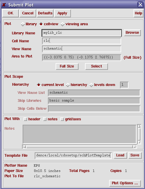
- Click on Plot Options... in the lower right hand corner of the window. You will be presented with the
Plot Options window as shown here.
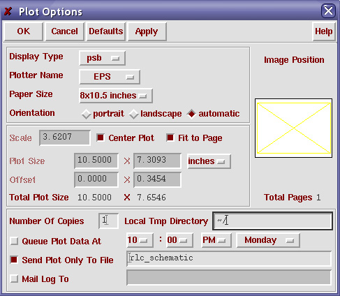
- Select the Plotter Type as EPS.
- Select the Paper Size as 8x10.5.
- Select the Send Plot Only to File option and enter the desired schematic name, i.e., rlc_schematic.
- Click on OK.
- Back in the Submit Plot window, click the OK button.
- The printed schematic, in EPS format, should now be located within your cadence directory.
Creating a Symbol View
You now need to create a Symbol view of your circuit. The symbol view is a black-box view that
describes a circuit or component as a box with only inputs and outputs visible.
- To create the symbol view, we will create the Symbol cellview from or schematic cellview.
- Select Design => Create Cell View => From Cellview... to automatically create the symbol. You will
be presented with Cellview From Cellview window shown here.
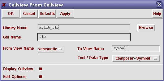
- Ensure From View Name is schematic and To View Name is symbol.
- Click on OK
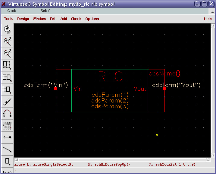
- You should be presented with the Symbol Editing Window.
- The outside red box defines the selection region region when selecting the symbol within a schematic design.
- The inside green box defines the dimension of the symbol as it would be shown within a schematic design.
- The cdsTerm("Vout") is a label that displays the pin names or the net names (Vout).
- The cdsParam(1,2,3) are labels that display parameters of an instance, e.g. 75 Ohm.
- The cdsName("") is a label that displays the instance or cell name, e.g. rlc1.
- Expand both the green and red boxes by selecting and drag the box edges.
- Relocate the input and output pins to the center of the expanded symbol.
- Relocate the cdsName items to the lower portion of the symbol.
- You should now add a label to the symbol to describe the symbol. Click on
the Label icon or select Add => Label. You will be presented
with the Add Symbol Label window shown here.
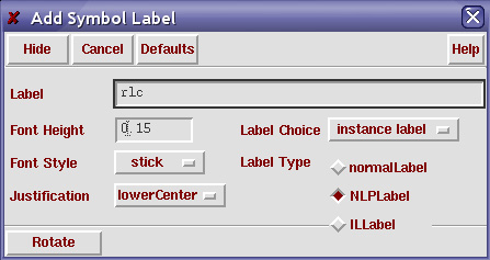
- Enter RLC as the Label.
- Change the Font Height to 0.15.
- Place the label inside the symbol within the Symbol Editing window. Your final
symbol should look similar to the following.
- Check and save the symbol view.
Creating a Test Circuit (Schematic)
Yo now need to create a schematic that will be used to test your circuit design.
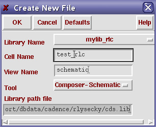
- From the Library Manager Window, select File => New => Cell View.
- Select mylib_rlc from the Library Name drop-down menu.
- Enter the cell name test_rlc in the Cell Name field as shown here.
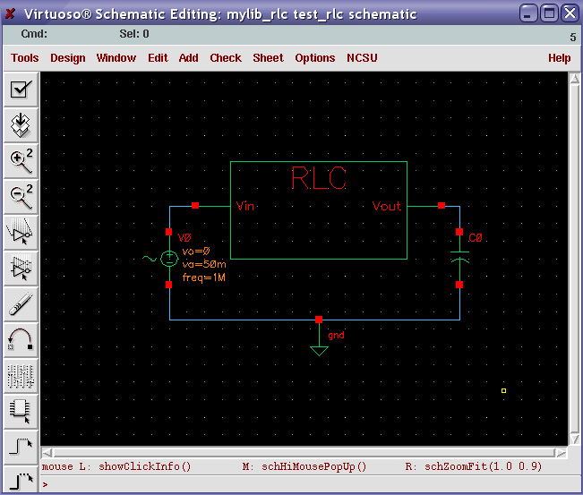
- First, you must add will add the RLC component you just create. Click on the
Instance icon or select Add => Instance.
- Again, you will be presented with two windows, the Component Browser and the Add Instance windows.
- From the Component Browser Window, under Library, select mylib_rlc.
- Select the component rlc from the list and place the component within your test schematic.
- From the analogLib library, add a vsin component.
- Before adding the component to your design, set the AC Magnitude to 1 V.
- Set the Offset Voltage to 0 V.
- Set the Amplitude to 50m V.
- Set the Frequency to 1M Hz.
- Add a 1p F capacitor, cap, and Ground, gnd to the test schematic and
connect the test schematic as shown here.
- Select Add => Wire Name.... You will be presneted with the following window.

- In the Name field enter Vin Vout.
- Switching back to the Schematic Editing window of your test circuit, add the wire names
to the circuit by selecting the wires connected to the input Vin and output Vout
of the RLC component.
- Your final test circuit schematic should look similar to the following.
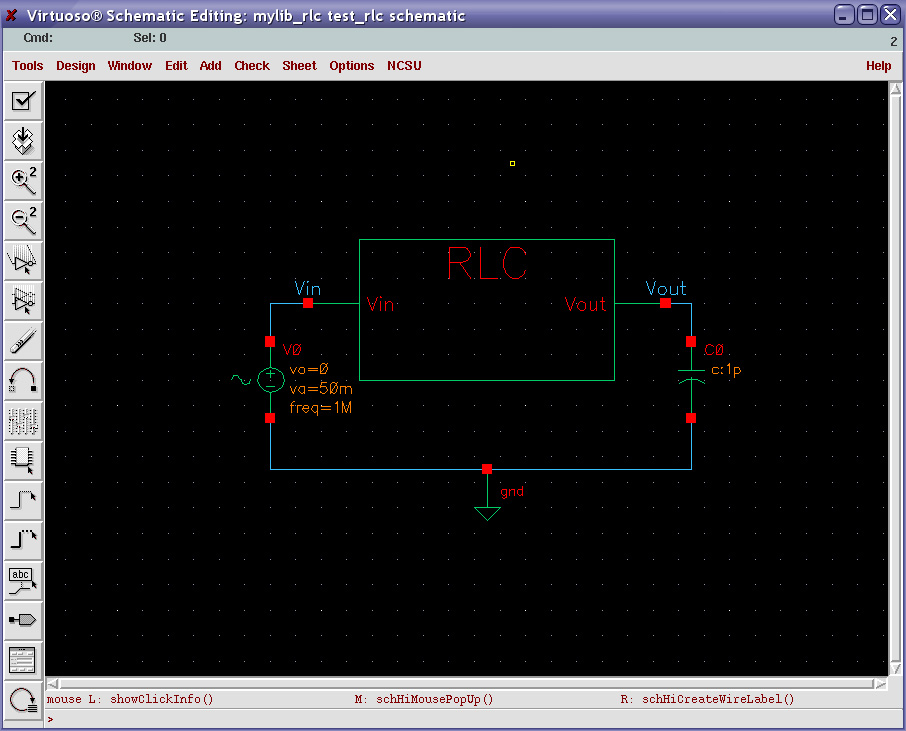
- Check and save the test circuit schematic.
Initializing the Simulation Environment
Using the test schematic you just created, you now will simulate your circuit design
using Cadence's Anolog Environemnt. For most of the labs, you will use a similar procedure to simulate
the schematic and layout designs you will create. The following provides an overview of the procedure required to
simulate a schematic design.
- From the schematic window of your test circuit, select Tools => Analog Environment.
- You will be presented with the Affirma Analog Environment window as shown here.
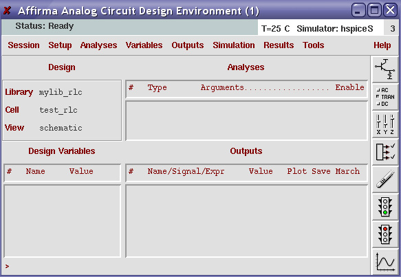
- The design area should indicate which schematic you are simulating, which is most cases should be the
schematic view of your test circuit.
Simulation Engine
There are many different simulation engines. For this coruse will we be using the SpectreS
simulation engine.
- In the analog environment window, select Setup => Simulator/Directory/Host.
- You should be presented with the window shown here.
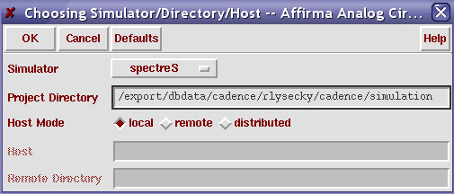
- Select the Simualator as spectreS
- Ensure the Project Directory is ~/cadence/simulation.
- Click on the OK button.
- If you are prompted to "Save Current State," select Yes and enter the state name as state1.
Choosing Analyses
In addition to different simulation engines, there are also different types of analyses. The following
is a brief breakdown of the different analyses available.
- Transient Analysis: This provides the transient output response of the circuit
with respect to time. The user specifies the time period and the time variant input waveform
while the simulator calculates the output response.
- AC Analysis: This simulates the AC performance of the circuit as a function of frequency,
and is based upon the small-signal frequency response model.
- DC Operating Point: This analysis simply determines the D.C. operating point of the circuit
based on the parameters present on the schematic assuming all capacitors opened and all inductors
shorted. It is the default mode and is automatically performed before any other analysis in order
to determine the initial state of the circuit.
- DC Sweep Mode: This generates DC transfer characteristics for the circuit by varying a user
specified independent source over a range of values.
For this lab we will using three of the available analyses types to simulation the circuit.
- Click on the Choose Analysis icon, or select Analysis => Choose.
- In the window that appears, select the Analysis as tran/. You should now be presented with the following
window.
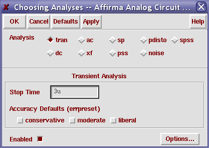
- In the Stop Time field, enter 3u.
- In the lower left hand corner, ensure that Enabled is selected.
- Click on the Apply button. By selecting Apply instead of OK, you can continue to
add more analyses without reopening the window. If you were to click OK, instead the Choosing Analyses
window will be closed.
- We now need to add an AC analysis. To do so, first select the Analysis as ac.
You should be presnted with the following window
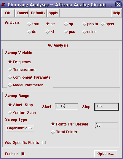
- Set the Sweep Variable to Frequency.
- Set the Sweep Range to Start-Stop.
- Set the Start to 0.01k.
- Set the Stop to 10k.
- Set the Sweep Type to Logarithmic.
- Set the Points Per Decade to 20.
- In the lower left hand corner, ensure that Enabled is selected.
- Click on the Apply button.
- We now need to add an DC sweep analysis. To do so, first select the Analysis as dc.
You should be presnted with the following window
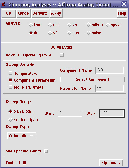
- Set the Sweep Variable to Component Parameter.
- Click on the Select Component button. At this point you shoul dswitch to your
test schematic window and click on the vsin component you added earlier.
- You will then be presented with the Select Component Parameter window shown here.
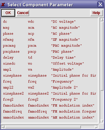
- Select the component parameter dc and click the OK button.
- Back in the Choosing Analyses window, set the Sweep Range to Start-Stop.
- Set the Start to 0.
- Set the Stop to 100.
- In the lower left hand corner, ensure that Enabled is selected.
- As we are finished adding analyses, you can click on the OK button.
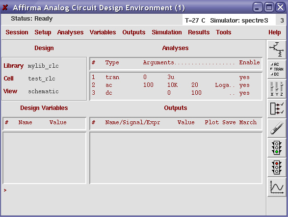
- Your Affirma Analog Environment window should look similar to the following.
Plotting Simulation Data
Before you can simulate the design, we first need to select which signals, inputs, and
outputs you want to simulate. While there are several methods that you can use to select the
simulation outputs, the most convinient method is described here.
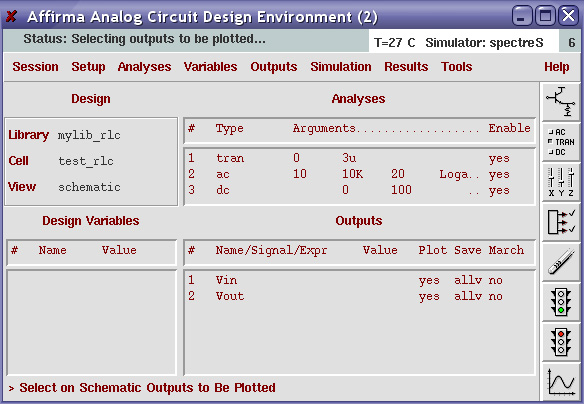
- Select Outputs => To Be Plotted => Select on Schematic.
- You should now swich back to your Schematic Editing window of your test circuits
and select the wires you previously labeled Vin and Vout.
- Your Your Affirma Analog Environment window should look similar to the following.
Running the Simulation
We can now simulate our design and view the simulation output to ensure proper functionality.
- Click on the Run Simulation icon or select Simulation => Run.
- You will be presented with the Waveform Window as shown here.
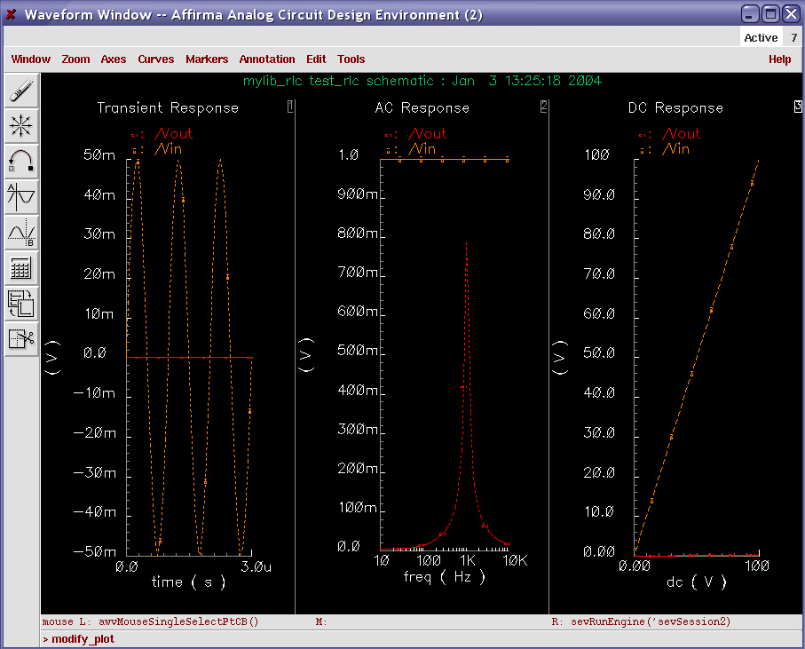
- The waveform window consists of three separate plots for each of the three analyses you selected.
you can switch between the different plots by clicking within the plot area. Select the DC Response
plot. You should notice the 3 in the upper right corner of the plot is highlighted, indicating
which plot is currently selected.
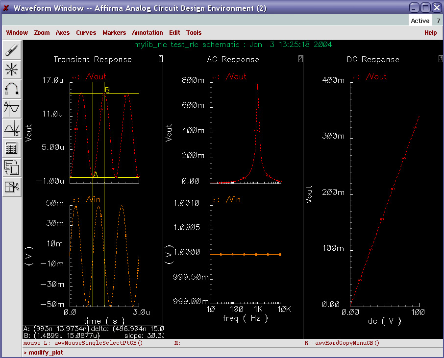
- Select Axes => to Strip. This will split the waveform for the DC Response into
two separate plots for Vin and Vout. Repeat this process for the other two analyses.
- Double-click on the y-axis label of the Transient Response. The following window
will be shown.
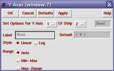
- Fill in the Label field with Vout and click on OK. Repeat this process for
the other plots.
- Use the Markers (A, B) to measure the output peak-to-peak amplitude of the Transient Response signal.
Click on the Crosshair Marker A icon on the left. Click on a negative peak of the output
waveform. Repeat for Crosshair Marker B, selecting the negative peak.
- The information for each marker, along with the delta (difference) between the two will be displayed
at the bottom of the plot.
- We can also delete waveforms from the waveform window. To delete the bottom Vin-Vin plot of
the DC Response section, click on the bottom waveform, and press the Del key on your keyboard.
- At this point, your Waveform Window should look similar to the following.
Printing the Simulation Waveform
To print the simulation results, use the following procedure.
- Select Window => Hardcopy. You will be presented with the Hard Copy window as shown here.
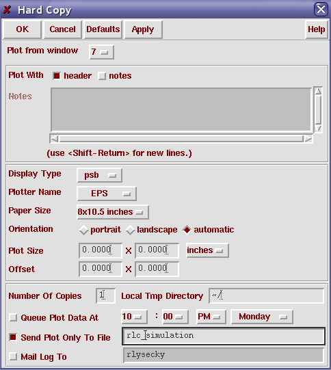
- Select the Display Type as psb.
- Select the Plotter Type as EPS.
- Select the Paper Size as 8x10.5.
- Select the Send Plot Only to File option and enter the desired schematic name, i.e., rlc_simulation.
- Click on OK.
- The printed waveform, in EPS format, should now be located within your cadence directory.
Congratulations
Congratulations, you have now successfully created a schematic design and simulated
that design to ensure proper functionality.
Demo
You must demo the following aspects or your NAND gate design to the TA.
- RLC schematic design.
- RLC test circuit schematic design.
- RLC simulation results.
Lab Report
In addition to the standard lab report format, you must submit the following information.
- Circuit schematic.
- Circuit symbol view.
- Test circuit schematic.
- Circuit simulation waveform.