GATE: width 3.6 length 0.6
·
Design > Save nmos
3.
Creating a pmos divice
File—Open
Or Tools>Library
Manager
Library Name design
Cell Name pmos
View Name layout
Virtuoso Layout Editor (VLE) Overview
Zooming In
and Out
Selecting
shapes
Drawing
shapes – Draw nmos and pmos devices
Editing
shapes
Placing an
instance
Creating
pins
Editing the
properties of objects
Using path
stitching
1.
Opening a layout and review commands
cd layout
layoutPlus & (calls up the Cadence
tools)
In the CIW, select File—Open, then enter the following values
in the form:
The
Following are basic editing commands that can be accessed from the pull down
menus or your bindkeys.
·
Options > Display = “e”
The Options form allows you change your layout environment
i.
Select the Axis to be on
ii.
Snap Mode change to orthogonal for
Create and Edit
·
Pan = Tab>LMB
·
Zoom In =
“z”
·
Zoom in by 2 =
“^z”
also RMB then window area
·
Zoom Out =
“Z”
·
Select =
“a”
to select 1 item
·
Select = hold “a”
to select more that one item
·
Area Select = “a”
> LMB to window area
·
Deselect =
“^d”
·
Fit View =
“f”
·
Redraw= “^r”
·
Create Rectangle = “r”
·
Create Path =
“p” Can do Path stitching the lets you
place contacts or vias according to what layer you need to jump up/down to.
·
Stretch =
“s”
use F4 to Partial Select to stretch a polygon side
·
Copy = “c”
·
Move = “m”
·
Create Ruler =
“k”
·
Delete Ruler = “K”
·
Placing an Instance =
“I”
·
Edit>Properties
= ”q”
·
Create Pins = “^p”
·
Create contact= “c”
·
View Stop Level 0 = “^f”
·
View Stop Level All = “F”
·
Layer Tap = “t” shows you what layer it taped by
highlighting that layer in the LSW.
·
ESC gets you out of a command you will us this often
·
F4 Toggles between Full Select and Partial Select (In
banner see Select)
·
LSW = Layer Select Window
·
Turns on/off Viewable and
Selectable for Layers, Instances and Pins
2.
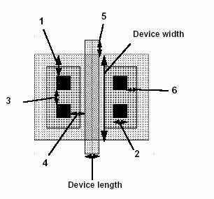
Creating an nmos device
File—Open
Or Tools>Library Manager
Library Name design
Cell Name nmos
View Name layout
Using
the following Design Rules to create the nmos device by using the commands
above
1. ndiff overlap of contact 0.9u
2. contact minimum width 0.6u
3. contact spacing 0.6u
4. contact to gate spacing 0.6u
5. poly extension 0.6
6. metal overlap of
contact 0.4u
GATE: width 3.6 length 0.6
·
Design > Save nmos
3.
Creating a pmos divice
File—Open
Or Tools>Library
Manager
Library Name design
Cell Name pmos
View Name layout
1. nwell overlap of pdiff 0.4u
2. pdiff overlap of contact 0.9u
3. contact minimum width 0.6u
4. contact spacing 0.6u
5. contact to gate spacing 0.6u
6. poly extension 0.6u
7. metal overlap of contact 0.4u
GATE: width 7.2 length 1.0
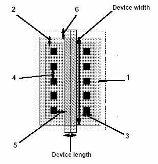
·
You can start from scratch or copy nmos cell into your
pmos cell.
·
Change ndiff to pdiff – Select ndiff Edit>Properties = ”q”
·
Using Edit > Properties continue with the poly length.
·
Use stretch, move and copy to match device width and
length and meet design riles.
·
To create nwell, select pdiff – Create > Layer
Generation – pdiff grow by 0.4 = nwell dg
·
Design > Save pmos
We will need to change the enclosure of
pdiff around contact to
0.5 micron,
and the metal1
enclosure around contact to be 0.4 micron.
Do the following to correct the pdif
enclosure of contact:
SymContactDevice( (name viaLayer viaPurpose layer1
purpose1 layer2 purpose2 w l (row column xPitch yPitch xBias yBias) encByLayer1 encByLayer2
legalRegion)
Note: A
PTAP contact contains the contact layer enclosed by two layers: pdiff and
metal1.
Loading the Edited Technology File
5.
Creating an Inverter with the nmos
and pmos devices already created.
Library Name design
Cell Name inverter
View Name layout
1. Cell height 18.0u
2. Width power and ground 1.8u
3. ndiff to pdiff spacing 0.5u
4. metal1 to metal1 spacing 0.8u
5. metal1 width 0.8u
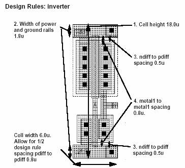
·
pwr and gnd rail of 1.8u wide with the cell height of
18.0u is already placed.
·
Using “i”
instance to Place nmos and pmos devices
Create
Instance form appears. Fill in with the following:
Library Design
Cell nmos or pmos
View layout
·
Place device according to the design rules.
·
Add the PTAP/NTAP using the Create contact “c”
·
Design Save inverter (keep open)
6.
Creating Pins
There are pins on the schematic
for the input (A), output (Y), power (vdd) and
ground (gnd). The corresponding
pins must be placed in the layout in order
to add the connectivity to run
Virtuoso® Custom
Router, Assura™ Verification or Diva® LVS, Virtuoso®-XL layout editor, and layout synthesis
tools.
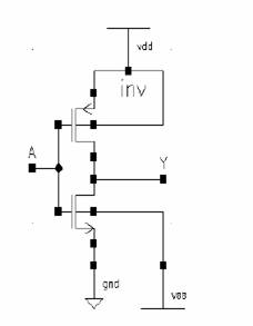
Fill out form like form below:
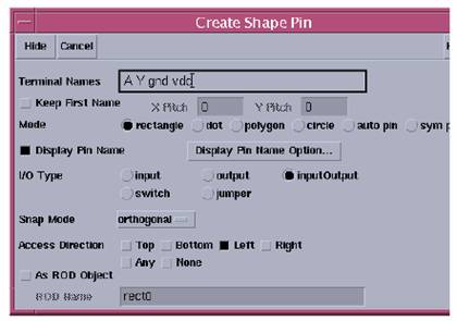
·
In LSW select Poly pn, Pin A will be on Poly
·
Pin Y gnd and vdd will be on metal1
·
The Pin rectangle must be enclosed by the layer it is
placed on.
·
Design Save inverter
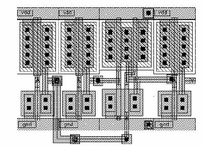
7.
Creating the control Block
File—Open
Library Name design
Cell Name control
View Name layout
Then open the corresponding
schematic named control schematic.
The inverter is what you have
created, the nand has already been created. Using the commands you used
previously place these instances and route the nest.
Try using
Path to do Path Stitching.
You will
also have to add pins to this level.